File name
File description

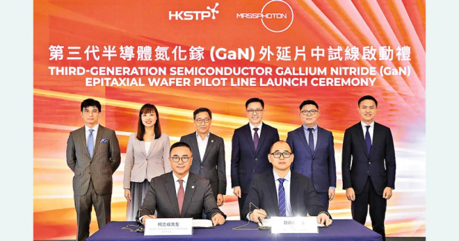
July 30, according to Hong Kong media sources, the Hong Kong Science and Technology Parks Corporation (HKSTP) and Massachusetts Photonics Technologies (Hong Kong) Limited (MassPhoton) successfully signed a cooperation agreement to set up Hong Kong's first third-generation semiconductor Gallium Nitride Epitaxial Process Global Research and Development Center within the Hong Kong Science Park, and to open the first Ultra-High-Vacuum mass-production Gallium Nitride Epitaxial Wafer Pilot Line in the InnoCentre. By 2027, we aim to achieve a production capacity of 10,000 wafers.
Gallium Nitride (GaN) is one of the main representative materials of third-generation semiconductors, featuring wide bandwidth, high frequency, low loss, strong radiation resistance and excellent breakdown electric field, which can be operated for long periods of time at high temperatures and high voltages, and has been widely used in LEDs, lasers, solar batteries, wireless communications, fast-charging, industrial and automotive applications.